BTC $80,841.36 +1.41%
ETH $2,350.58 +1.73%
BNB $744.99 +1.14%
XRP $1.33 +2.33%
SOL $101.85 +1.85%
TRX $0.3308 +0.76%
DOGE $0.0795 +2.69%
ADA $0.2062 +1.03%
BCH $297.63 +6.32%
LINK $11.74 +3.32%
HYPE $81.51 +5.20%
AAVE $134.44 +1.46%
SUI $0.9356 +2.95%
XLM $0.1715 +2.29%
ZEC $1,312.14 +7.31%
AAPL $346.73 +1.00%
AMZN $254.33 +2.29%
GOOGL $325.12 +2.03%
MSFT $530.24 -0.18%
META $621.62 -1.79%
NVDA $218.82 +1.31%
TSLA $409.13 +4.24%
SNDK $1,364.43 +8.10%
INTC $95.43 +5.80%
SPCX $150.06 +1.74%
MU $969.32 +6.26%
AMD $570.03 +7.63%

hbm4

All
Article
Flash

first_img SK Hynix's partial HBM4 backend equipment orders may be postponed until next year

According to DealSite, storage chip manufacturer SK Hynix is expanding the mass production of the sixth-generation high bandwidth memory HBM4. However, some industry insiders believe that the expansion speed is slower than expected, and some equipment orders planned for this year may be postponed until next year.Industry insiders stated that some equipment originally scheduled for delivery in the second half of this year has shown signs of delay, and subsequent order plans have not yet been clarified. An anonymous source indicated that some equipment originally planned for this year may be pushed to next year, and there is no data confirming whether the delivered equipment is operating at full capacity. The investment plans related to HBM4 for next year have not been specifically communicated to some partners, and this year's orders have largely been completed, but there are no clear signals of increased or decreased investment. Reports suggest that the direct correlation between the equipment investment schedule and product quality issues has not yet been confirmed.Liu Henggen, a researcher at Daxin Securities, believes that concerns about major customers' HBM4 quality issues leading to performance below expectations are excessive. There may have been some issues in the backend process, but they cannot be regarded as insurmountable risks, and it is not yet time to discuss bad compensation. There are also industry claims that, against the backdrop of rising prices for general memory, some HBM investments may shift towards general memory. SK Hynix plans to prioritize the introduction of DRAM production equipment into the first cleanroom of the Yongin cluster Y1 wafer fab, and the industry expects that the initial production line will adopt the sixth-generation 10-nanometer 1c process, with the new capacity being prioritized for general DRAM. Some opinions also suggest that changes in the schedule of certain backend equipment are insufficient to determine that HBM4 mass production is hindered, as SK Hynix has already supplied HBM4 16-layer samples to major customers.

first_img Samsung and SK Hynix respond to HBM4E heat dissipation, AI intermediary layer may expand to 40 times

TrendForce reported on October 12, citing Chosun Biz, that as AI packaging accommodates more computing and storage chips, the intermediary layer connecting computing chips and HBM is expected to significantly increase in size, making next-generation HBM cooling more important. Samsung Electronics is preparing multiple technologies to address the cooling challenges of HBM4E, which is scheduled to begin mass production next year.Currently, the area of the AI intermediary layer is about 5.5 times the maximum exposure area of 858 square millimeters of an EUV lithography machine. Semiconductor equipment industry insiders expect that the intermediary layer carrying HBM could expand to 9 times, 12 times that area, and ultimately about 40 times. Reasons include limitations in process miniaturization and the popularity of chiplet-style 2.5D packaging, where multiple computing chiplets and HBM stacks are placed on the same intermediary layer, making it difficult for a single advanced process chip to meet AI computing power demands.Samsung is considering hybrid copper bonding and thermal path blocks. The former replaces the micro bumps between stacked DRAM chips with direct copper-to-copper connections, which can reduce inter-layer gaps, make the stack thinner, and improve heat dissipation, a technology Samsung showcased at NVIDIA GTC in March 2026. The thermal path block establishes a dedicated thermal path in the D2D PHY area responsible for high-speed transmission between HBM base chips and GPUs, which Samsung is validating with HBM4E and plans to implement in HBM5. According to ETNews, SK Hynix's iHBM places high thermal conductivity but electrically insulating cooling materials around the heat-concentrated D2D PHY, which is expected to reduce thermal resistance by about 30%.

first_img Samsung Electronics plans to expand production of 4-nanometer to meet HBM4 demand

According to Money Today on September 21, Samsung Electronics is advancing the expansion of advanced process capacity in wafer foundry due to the growth of the HBM market. To meet the rising demand for HBM4 base chips, it is evaluating the expansion of its 4-nanometer process. Samsung's HBM4 consists of 10-nanometer 6th generation (1c) DRAM core chips and 4-nanometer logic base chips, with the base chips responsible for high-speed data exchange with AI accelerators such as GPUs.Unlike SK Hynix, which uses TSMC's 12-nanometer process for HBM4 base chips, Samsung employs its own 4-nanometer process. This production line is operating at full capacity and has taken on orders from companies like Nvidia and Groq for 3 LPU, and the company has recently raised its prices for new 4-nanometer orders and HBM4 base chips. Samsung expects HBM4 revenue in the third quarter to increase more than threefold quarter-on-quarter, with HBM4 accounting for significantly more than 60% of HBM revenue in the second half of the year. The additional expansion at P4 in Pyeongtaek will mostly be used for 1c DRAM for HBM, with more than half of the wafer foundry's 4-nanometer capacity allocated to HBM4 base chips.HBM4E also uses 4-nanometer base chips, and Samsung provided samples to customers in May. The company is also evaluating the construction of a new 2-nanometer production line for HBM5, aiming for a GAA structure 2-nanometer process and increasing TSV density to improve operating speed by more than 50% compared to HBM4E. Samsung started the first generation of 2-nanometer mass production in the second half of last year and is advancing the second generation of products in the second half of this year. Citigroup expects global HBM bit demand to reach 75.2 billion Gb next year, a year-on-year increase of 62%, with supply around 59.4 billion Gb and a gap of about 21%.

first_img Samsung's 4-nanometer production capacity is more than half used for HBM4 substrate chips

Samsung Electronics' wafer foundry division has recently surpassed 50% in the allocation of production capacity for the sixth-generation high bandwidth memory HBM4 substrate chips in the 4-nanometer process. The industry states that this division will invest more than half of its 4-nanometer wafers into HBM4 substrate chip manufacturing in the second half of this year to expand supply to companies like NVIDIA, Broadcom, and AMD.Samsung initiated mass production and shipment of HBM4 in February this year and plans to increase supply starting from the third quarter, significantly increasing the related wafer input since mid-year. This chip is based on Samsung's wafer foundry 4-nanometer (SF4) process. As of last month, over 50% of its total 4-nanometer capacity has been allocated to HBM4 substrate chips. According to insiders, Samsung's 4-nanometer process is currently at full capacity, with HBM4 substrate chips accounting for about 50% to 60%, and this high proportion will be maintained in the second half of the year.Samsung's wafer foundry production lines at Pyeongtaek Plant 2 and Plant 3 are mass-producing processes ranging from 4 to 7 nanometers, with a monthly capacity of about 30,000 wafers for the 4-nanometer process. Based on this, the wafer input related to HBM4 substrate chips is estimated to be about 15,000 wafers per month. During the second quarter earnings call, Samsung stated that it expects HBM4 revenue to increase more than threefold quarter-over-quarter in the third quarter, with HBM4 revenue in the second half expected to exceed 60% of the company's overall HBM revenue.

first_img Samsung develops NVIDIA's custom NVHBM to advance 8-layer high-speed HBM4E

According to reports from Seoul Economic Daily, Samsung Electronics is developing HBM4E (seventh generation) 8-layer products that meet NVIDIA's requirements, aiming to secure its position as a core partner in the supply of customized high-bandwidth memory NVHBM. This product reduces the stacking height compared to the originally planned 12-layer and 16-layer designs. The speed specifications proposed by NVIDIA are 17-18Gbps, which is about 20% higher than the speed of Samsung's initial HBM4E samples (14.4Gbps), and will be used for NVIDIA's publicly disclosed NVLink optimized specifications for NVHBM.The use of 8 layers, contrary to the previous logic of increasing capacity by adding more stacking layers in HBM, can reduce the difficulty of post-processing and yield pressure, which is beneficial for expanding supply and is seen as NVIDIA's strategy to alleviate memory shortages. NVHBM is expected to be applied starting with the next-generation AI GPU "Rubin Ultra," which is set to launch next year. This GPU will expand the interconnection scale between GPUs from a maximum of 72 to 576, enhancing overall computing power through hundreds of GPUs equipped with faster HBM.In the customized HBM market, Samsung is more competitive compared to SK Hynix and Micron, as NVHBM requires DRAM and the production capabilities of logic chip-based bare die designs, which Samsung can integrate. Industry insiders say that Samsung has verified the highest speed levels in HBM4, which can provide an advantage in speed competition.

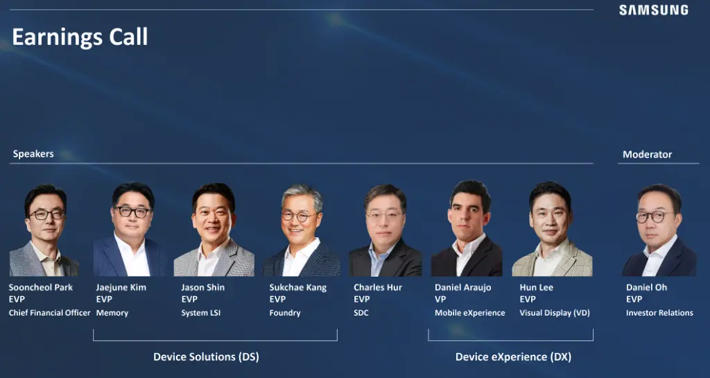
hot_img Samsung Electronics' Q2 revenue reached a record high of 171.5 trillion won, with operating profit soaring 1813% year-on-year to 89.5 trillion won

Samsung Electronics released its Q2 2026 financial report, with revenue of 171.5 trillion Korean won (approximately $118.8 billion), a year-on-year increase of 130%, and a quarter-on-quarter increase of 28%, setting a new record for a single quarter; operating profit was 89.5 trillion Korean won (approximately $62 billion), a year-on-year increase of 1813.8%, and a quarter-on-quarter increase of 56.4%, exceeding market expectations by about 5%; net profit was 71.62 trillion Korean won (approximately $49.6 billion), a staggering year-on-year increase of 1299.9%. Earnings per share were 10,849 won, a year-on-year increase of 52%.The Device Solutions (DS) division reported revenue of 127.5 trillion Korean won, with operating profit of 89.2 trillion Korean won, a quarter-on-quarter increase of 56%, driven by demand for AI server memory, with both revenue and profit reaching historical highs. HBM4 has been mass-produced and shipped, and HBM4E samples have been delivered to major customers. The Device Experience (DX) division saw a quarter-on-quarter revenue decline of 9%, with the MX business affected by component cost pressures, reporting revenue of 33.2 trillion Korean won and an operating loss of 0.7 trillion Korean won.Samsung expects strong demand for server DRAM, eSSD, and HBM to continue in the second half of the year, with a tight market supply situation persisting, although demand in the mobile and PC sectors may see some slowdown. The company plans to expand sales of high-value-added products such as HBM4, DDR5, and SOCAMM2, and to mass-produce new mobile products using the second-generation 2nm process, aiming for double-digit revenue growth in its foundry business.
app_icon
ChainCatcher Building the Web3 world with innovations.