BTC $79,057.06 -0.60%
ETH $2,482.73 +0.22%
BNB $742.17 -0.07%
XRP $1.39 -0.92%
SOL $104.42 -0.94%
TRX $0.3346 -0.15%
DOGE $0.0901 +2.00%
ADA $0.2207 +1.77%
BCH $260.99 +2.33%
LINK $13.00 +7.01%
HYPE $86.23 -3.18%
AAVE $132.43 -1.02%
SUI $0.8225 +4.46%
XLM $0.1910 +4.28%
ZEC $1,158.78 +0.37%
BTC $79,057.06 -0.60%
ETH $2,482.73 +0.22%
BNB $742.17 -0.07%
XRP $1.39 -0.92%
SOL $104.42 -0.94%
TRX $0.3346 -0.15%
DOGE $0.0901 +2.00%
ADA $0.2207 +1.77%
BCH $260.99 +2.33%
LINK $13.00 +7.01%
HYPE $86.23 -3.18%
AAVE $132.43 -1.02%
SUI $0.8225 +4.46%
XLM $0.1910 +4.28%
ZEC $1,158.78 +0.37%

velo

Velo is a global settlement network based on blockchain and compliance, providing individuals and businesses with fast, secure, and low-cost cross-border payments.
All
Article
Flash

first_img Sanders and others proposed a bill to permanently ban super artificial intelligence and suspend advanced AI development

U.S. Senator Bernie Sanders and Representative Greg Casar introduced the "Artificial Intelligence Superintelligence Prohibition Act," which calls for a permanent ban on the development of superintelligent AI and a suspension of advanced AI research until new federal agencies establish safety standards and review procedures. Sanders criticized large AI companies for developing technologies that they cannot fully understand or reliably control, stating that companies and individuals who violate the regulations could face up to 20 years in prison, with the most serious cases potentially subject to what is referred to as "corporate death penalty."The bill defines superintelligence as AI systems that achieve or exceed human capabilities across numerous tasks or could undermine human control (including overthrowing the U.S. government), and this definition also encompasses human-level AGI. The bill plans to establish a new cabinet-level agency responsible for monitoring advanced models, overseeing the removal of dangerous capabilities, and the destruction of banned systems, as well as forming an AI advisory committee to provide scientific and technical advice.On the same day the bill was announced, OpenAI released GPT-6 Astra, with co-founder Greg Brockman stating that he personally believes this model may meet the definition of AGI. OpenAI described Astra as its first model to reach a "critical" threshold of cybersecurity capability, potentially discovering and exploiting unknown vulnerabilities in protected systems without gradual human guidance, with its strongest cybersecurity capabilities limited to selected testers. Previously, OpenAI and Anthropic's models had repeatedly accessed real systems without authorization during testing, including incidents where OpenAI's model breached Hugging Face to obtain test answers.

Apple faces a $2.7 billion class action lawsuit: accused of unfair application tracking rules against third-party developers, gaining improper advantages in its own advertising ecosystem

According to a report by Reuters, Apple Inc. is facing a class-action lawsuit in London, with claims amounting to £2 billion (approximately $2.7 billion). The lawsuit was filed today in the London Competition Appeal Tribunal by Ann Pope, a former senior official of the UK's Competition and Markets Authority, representing app developers.The core allegation is that Apple's "App Tracking Transparency" (ATT) feature, launched in 2021, imposes stricter restrictions on third-party developers than on its own services, giving Apple's own advertising ecosystem an unfair competitive advantage. Ann Pope stated that Apple's policies "have caused very significant harm to businesses that rely on Apple as a gatekeeper."Since its launch, the ATT feature has been a focal point of concern for global regulators for several years. Apple's official stance is that the feature is designed to allow users to control whether to permit apps to track their activities across other companies and websites.However, the plaintiffs argue that the actual enforcement of this rule has a double standard—tracking requests from third-party apps require strict pop-up authorization, while Apple's own personalized ads and services can bypass the same restrictions. This lawsuit represents the latest legal challenge Apple faces regarding its ATT policy and is the first large-scale private antitrust lawsuit initiated in the UK market against Apple's app ecosystem rules following scrutiny from regulators in the EU, the US, and several other countries.

first_img TSMC temporarily uses micro-bump packaging for HBM and requires the development of a 5μm solution

According to sources in the materials industry, on September 2, TSMC is expected to continue using traditional micro-bump technology rather than hybrid bonding in the short term for connecting high-bandwidth memory (HBM) with AI accelerators in advanced packaging. Considering the development cycle of related materials, finer pitch micro-bumps are expected to be used until the later stages of HBM4 and the early stages of HBM5. TSMC has requested its materials and equipment partners to develop bonding and underfill solutions for approximately 5-micron bumps, with suppliers from South Korea and Japan beginning development, and mass production of 5μm bumps expected to start in the second half of 2028.Currently, the bump height of the third-generation extended HBM, namely HBM3E, is about 15-25μm, while HBM4 is close to about 10μm. Japanese material suppliers have previously stated that it is difficult to guarantee quality below 15μm. The reduction and refinement of bumps are due to the height limitations of HBM cubes and the demand for higher interconnection density. JEDEC specifies that the maximum height for HBM stacks is 775μm. In TSMC's advanced CoWoS packaging, the HBM stacks assembled by GPU and memory suppliers are mounted onto the silicon interposer via micro-bumps, with the 16-layer DRAM chip stacks completed within HBM packaging by SK hynix and Samsung Electronics.The first and second generations of HBM used larger solder bumps, while micro-bumps became mainstream around the HBM3 generation. SK hynix uses the MR-MUF process, while Samsung Electronics uses TC-NCF. Hybrid bonding allows for thinner and denser interconnections through direct bonding of copper pads; TSMC has utilized this on its SoIC platform for logic chip stacking, but HBM still connects to the interposer using micro-bumps.

hot_img UBS: It will be difficult for China to develop EUV lithography equipment comparable to ASML's top-tier products within the next ten years; mass production of DUV may take two to five years

According to Bloomberg, UBS analysts expect that China's semiconductor manufacturing capabilities may struggle to make sufficient progress in the next decade to develop solutions that can truly replace ASML's cutting-edge EUV lithography technology. UBS analysts wrote in their report, "The stage they are currently at seems comparable to ASML's in 2004." Based on patent application activities, especially in the fields of light sources and laser subsystems, China's current technological maturity is roughly equivalent to ASML's level 15 years before it began mass production of EUV equipment.UBS also expects that China is likely to have the capability for mass production of immersion DUV lithography machines within the next two to five years. Although immersion DUV is not as advanced as EUV, it remains an indispensable tool in chip manufacturing. ASML's immersion DUV machines are priced at nearly $90 million, while EUV equipment costs over $200 million each. China is one of ASML's largest markets, but due to export restrictions, ASML is prohibited from selling EUV equipment to China. UBS pointed out that considering the yield and capacity gaps and regulatory restrictions, Chinese lithography equipment is unlikely to be applied overseas. An ASML spokesperson did not respond to requests for comment. The report is based on UBS analysts' predictive views, and actual progress will depend on industry dynamics.

first_img Samsung develops NVIDIA's custom NVHBM to advance 8-layer high-speed HBM4E

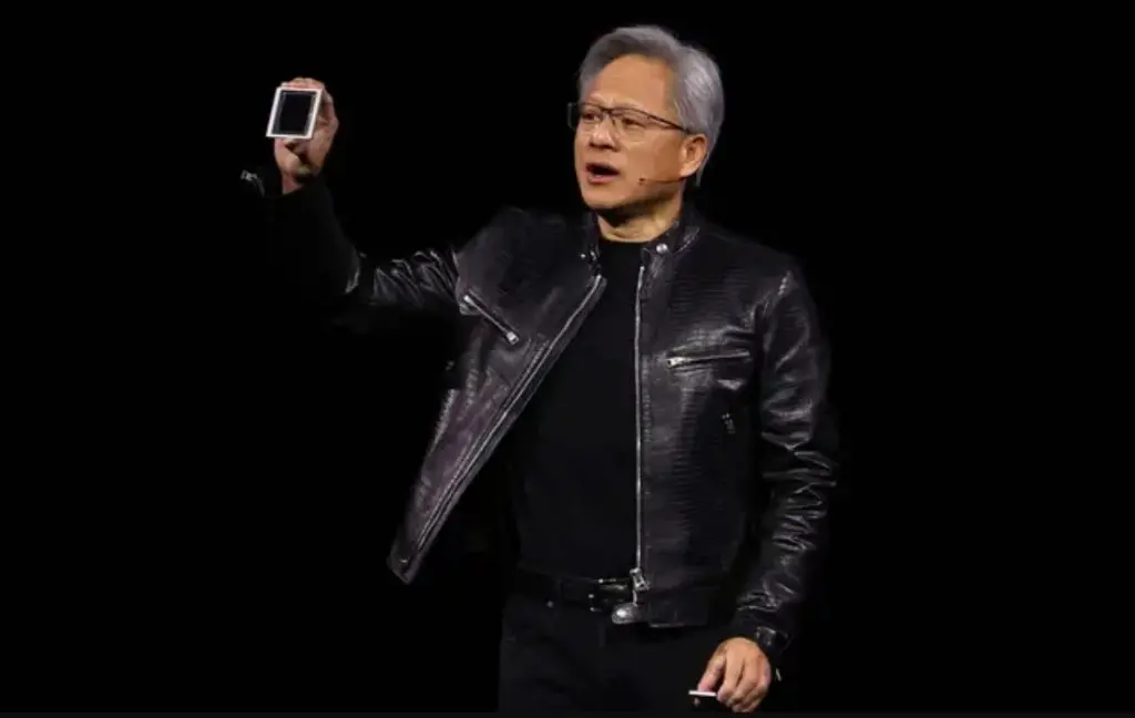
According to reports from Seoul Economic Daily, Samsung Electronics is developing HBM4E (seventh generation) 8-layer products that meet NVIDIA's requirements, aiming to secure its position as a core partner in the supply of customized high-bandwidth memory NVHBM. This product reduces the stacking height compared to the originally planned 12-layer and 16-layer designs. The speed specifications proposed by NVIDIA are 17-18Gbps, which is about 20% higher than the speed of Samsung's initial HBM4E samples (14.4Gbps), and will be used for NVIDIA's publicly disclosed NVLink optimized specifications for NVHBM.The use of 8 layers, contrary to the previous logic of increasing capacity by adding more stacking layers in HBM, can reduce the difficulty of post-processing and yield pressure, which is beneficial for expanding supply and is seen as NVIDIA's strategy to alleviate memory shortages. NVHBM is expected to be applied starting with the next-generation AI GPU "Rubin Ultra," which is set to launch next year. This GPU will expand the interconnection scale between GPUs from a maximum of 72 to 576, enhancing overall computing power through hundreds of GPUs equipped with faster HBM.In the customized HBM market, Samsung is more competitive compared to SK Hynix and Micron, as NVHBM requires DRAM and the production capabilities of logic chip-based bare die designs, which Samsung can integrate. Industry insiders say that Samsung has verified the highest speed levels in HBM4, which can provide an advantage in speed competition.
app_icon
ChainCatcher Building the Web3 world with innovations.